FAB ACADEMY 2017
Week 6 - Electronics Design
Electronics Design
The main conclusion about this week is that I feel ready to start exploring and trying to design my own boards. Mostly, i’m very motivated to do so. By embracing this task I understood how important it is to develop our own circuitry and how it turns our development process much more robust. I also used the week to explore other fabrication approaches, aiming at the use of a more low level CNC machine. (this specific process enriched my electronics production content, and will leave for a later tutorial.
Understanding the circuit
My first step was to understand the circuit and the changes that we were supposed to make. My previous experiences with Arduino (which I deeply recommend as front door to these worlds), helped me a to understand the potential of the Attiny, not only for this project as well for my final project. By a very simple analogy, we can just consider that all the PA pins, which are ADC pins can be connected as the simple circuits we connect to an arduino pin. Also, Previous year students, helped me get a clear view on what it was expected and what was the crystal meant to do. Again, by analogy with the AVR chips from Arduino, I soon understood that the internal time counting, impulses weren’t native from these smaller MCU’s. Also, the reset pullup resistor, declares the LOW state of the reset pin, which releases it from the float undefined mode. That does’n have to happen on an arduino AVR based system, because this MCU’s reset pins have internal pullup resistors.
Image from ATTINY44: datasheet

Eagle eyes over Eagle CAD
I started by a very quick and well structured “Ben Heck Show” tutorial on youtube, My first guess was: having explored it previously, adding the well structured content of the class and tutorship of Luís I could easily understand handle it. The first challenge was to replicate the helloBoard exactly as defined. This process enabled me to get acquainted with the dimensions and types of components, and drawing strategies. For that, a couple of past student tutorials were essential: Xavier Dominguez Edgar R. Aguilar Arenales
Draw the schematic
Every board begins with the circuit definition.
- First place the components you are expecting to use inside the layout area.
- Define the best positions for a clear understanding.
- And start connecting everyhing.
- When done, run ERC and switch to board mode.
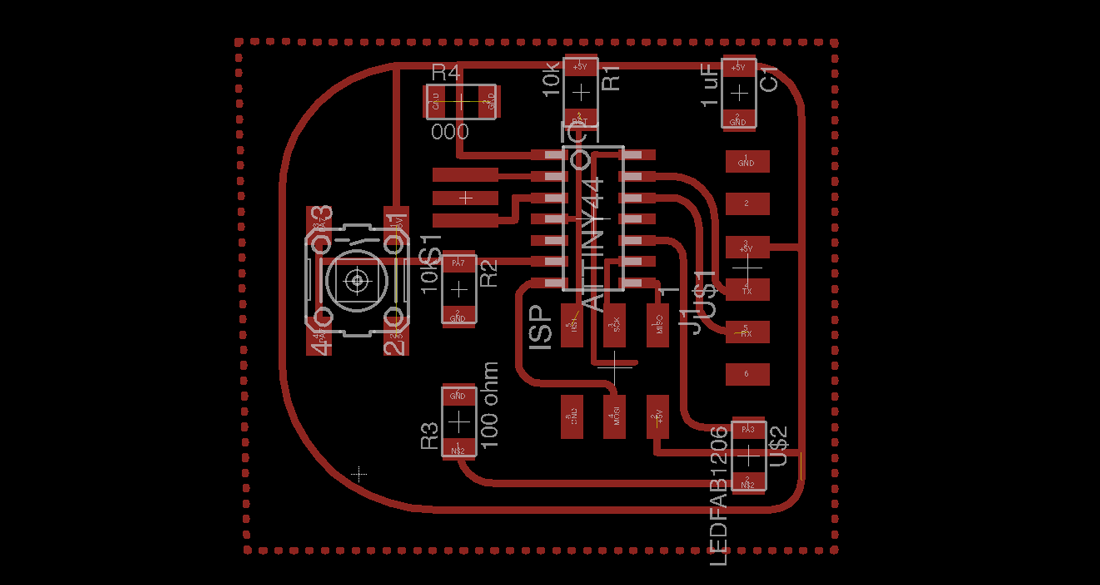
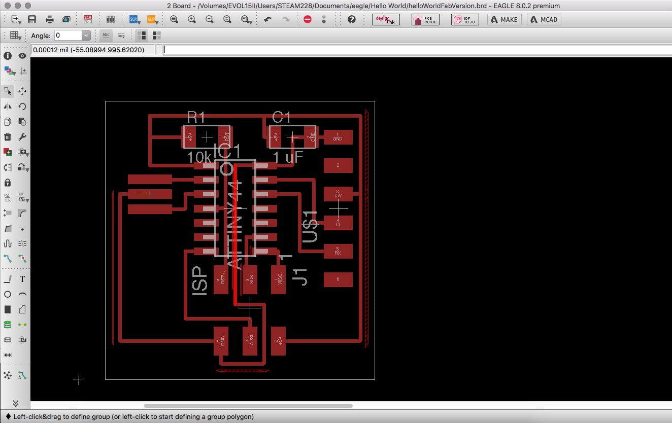
Design de Board
- By this time it is essential to understand part sizes
- And define a main trace sizes
- And start connecting everyhing.
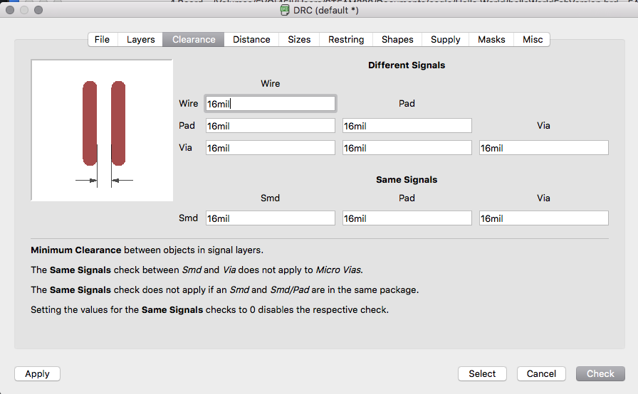
- Also your set of rules: Here you will be mainly worried about the clearance between conductive copper elements. If, like mentioned in most Eagle Tutorials, you are about to send the production files to a board house, then you should load their standards. In our case, we opted for 16 mil which is .4 mm, our smallest and most appropriate mill.
- Notice some hatch areas? It is, as a result of the test, one area where our mill would damage the circuit by cutting the trace.